[디지털 회로설계] 4-Bit D Flip Flop 설계


[디지털 회로설계] 4-Bit D Flip Flop 설계

디지털 회로설계
1. 제목 : 4-Bit D Flip Flop 설계
2. 개요 :
1) 목적 : 1 bit flip flop을 통해 4 bit flip flop을 VHDL과 logic gate로 설계한다. 이 과정에서 VHDL의 process의 사용법을 익히고, logic gate의 구현과 process로의 구현의 차이점을 비교해 본다.
2) 방법 :
[1-bit flip flop]
(1) 입력이 D, Preset, Clear, Clock이고 출력이 Q, notQ인 1 bit D F/F을 VHDL 언어로 설계한다.
(2) 위와 동일한 입출력을 가진 1 bit D F/F을 logic gate로 설계한다.
(3) 둘의 설계 과정과 결과를 비교해 본다.
[4-bit flip flop]
(4) 4 bit의 벡터 x, y와 carry in을 입력으로 갖고 4 bit의 벡터 s와 carry out을 출력으로하는 4 bit adder을 1bit adder 4개를 통해 설계한다.
(6) 설계한 4-bit full adder를 임의의 x, y 값을 입력하여 waveform을 출력한다.
3. 이론
(1) Half Adder
(2) Full Adder
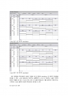
4. 설계과정
- 4-bit full adder의 truth table
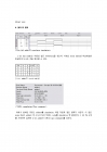
5. VHDL Code
[1-bit adder]
library ieee;
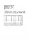
6. 결과 및 분석
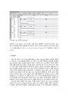
[1bit full adder의 waveform simulation]
1 bit full adder는 다음과 같은 waveform을 갖는다. 아래의 truth table과 비교해보면 동일하게 나오는 것을 확인할 수 있다.
cin
xy
cout
s00000001010100101110
[1 bit adder의 truth table]
....
1. 제목 : 4-Bit D Flip Flop 설계
2. 개요 :
1) 목적 : 1 bit flip flop을 통해 4 bit flip flop을 VHDL과 logic gate로 설계한다. 이 과정에서 VHDL의 process의 사용법을 익히고, logic gate의 구현과 process로의 구현의 차이점을 비교해 본다.
2) 방법 :
[1-bit flip flop]
(1) 입력이 D, Preset, Clear, Clock이고 출력이 Q, notQ인 1 bit D F/F을 VHDL 언어로 설계한다.
(2) 위와 동일한 입출력을 가진 1 bit D F/F을 logic gate로 설계한다.
(3) 둘의 설계 과정과 결과를 비교해 본다.
[4-bit flip flop]
(4) 4 bit의 벡터 x, y와 carry in을 입력으로 갖고 4 bit의 벡터 s와 carry out을 출력으로하는 4 bit adder을 1bit adder 4개를 통해 설계한다.
(6) 설계한 4-bit full adder를 임의의 x, y 값을 입력하여 waveform을 출력한다.
3. 이론
(1) Half Adder
(2) Full Adder
4. 설계과정
- 4-bit full adder의 truth table
5. VHDL Code
[1-bit adder]
library ieee;
6. 결과 및 분석
[1bit full adder의 waveform simulation]
1 bit full adder는 다음과 같은 waveform을 갖는다. 아래의 truth table과 비교해보면 동일하게 나오는 것을 확인할 수 있다.
cin
xy
cout
s00000001010100101110
[1 bit adder의 truth table]
....

-
[디지털 회로 설계] 4-Bit D Flip Flop 설계
디지털 회로설계 1. 제목 : 4-Bit D Flip Flop 설계 2. 개요 : 1) 목적 : 1 bit flip flop을 통해 4 bit flip flop을 VHDL과 logic gate로 설계한다. 이 과정에서 VHDL의 process의 사용법을 익히고, logic gat.. -
[디지털 시스템 설계 및 실험] Latch, Flip-Flop, Shift Register
디지털 시스템 설계 및 실험 결과보고서 실험제목 Latch, Flip-Flop, Shift Register 실험목표 1. SR NOR latch 2. Gated D latch(based on an SR NOR latch) 3. (Masterslave pulse-triggered) D flip-flop (wit.. -
 RS 및 D Flip Flop JK 및 T Flip Flop 발표 자료
RS 및 D Flip Flop JK 및 T Flip Flop Flip Flop 이란 플립플롭은 두 가지 상태 사이를 번갈아 하는 전자회로이다. 플립플롭에 전류가 부가되면,현재의 반대 상태로 변하며 (0 에서 1 로,또는 1 에서 0 으로), 그 .. -
[디지털 회로실험] 비동기 카운터
비동기 카운터 본 실험에서는 리플카운터의 기본형에 대하여 실험하고 모듈의 정의를 소개한다. 1. 서 론 비동기 카운터는 플립플롭을 직렬로 연결하여 구성하며 한 플립플롭의 출력은 그다음 플립플롭의 입력에.. -
[디지털공학] 플립플롭을 이용한 신호등 제어기 작성
목표 : 플립플롭을 이용한 신호등 제어기 작성. ◆ Flip-Flop 4bit동기 업 카운터를 만들기 위하여 JK F/F를 사용. ●FLIP FLOP-클럭 펄스가 나타나기 바로 이전의 입력이 출력에 반영되어 다음 클럭 펄스가 나타.. -
플립플롭(Flip-Flop)
◎ 플립플롭 대다수 놀리 회로들은 그들의 출력 값들이 현재 상태의 입력뿐만 아니라, 이전 상태의 값에 의해서 그 결과가 결정되는 성격을 갖는다. 이런 성격의 논리 회로들을 순차 회로라고 한다. 순차 회로.. -
[디지털 회로설계] 1-Bit Full Adder를 통한 4-Bit Full Adder 설계
디지털 회로설계 1. 제목 : 1-Bit Full Adder를 통한 4-Bit Full Adder 설계 2. 개요 : 1) 목적 : 1-bit full adder를 통한 4-bit full adder를 설계하여 adder에 대한 이해도를 높인다. N-bit adder로 확장하.. -
디지털 시스템 설계 및 실험 - 4bit Adder Subtractor
디지털 시스템 설계 및 실험 결과보고서 실험제목 ①4bit Adder Subtractor 실험목표 ①Half adder 와 Full-adder를 구성한다. ②Half adder 와 Full-adder를 이용하여 4bit Adder Subtractor를 코딩한다. 실험결과 .. -
디지털 공학 - 4bit 제곱기 설계
디지털 공학 -4비트 제곱기 설계 1) 블록도 2) 진리치표 입력 출력 ABCD수 Y0 Y1 Y2 Y3 Y4 Y5 Y6 Y7 값0001100011001020001004001130000100190100400010000 16 010150001100 ·1 25 0110600100100 36 0111700110.. -
[디지털 시스템 설계 및 실험] 4bit ripple counter
디지털 시스템 설계 및 실험 결과보고서 실험제목 Counter 실험목표 1. JK 플립플롭 제작 2. 4bit Ripple Counter 제작 실험결과 1. JK 플립플롭 제작 코딩module jk(J,K,C,Q,Q_); input J,K,C; output Q,Q_; wir..